Recently, I’ve passed a course on Coursera, which is called nand2tetris. The course itself is about building your own computer from the ground up. Though it will be better to quote the instructor himself, what the course is about:
The course guides students and self-learners through the construction of a modern, full-scale computer system - hardware and software - from the ground up. In the process, the students practice many major computer science (CS) abstractions studied in typical CS courses and make them concrete through 12 guided implementation projects.
And so, when I implemented the last module/project from the course, I got a Pong game, written in Jack language (your own language, implemented during the course).
Afterwards, the game is compiled through your own toolchain back into binary code and running on your own CPU. Both toolchain and CPU developed during the course.
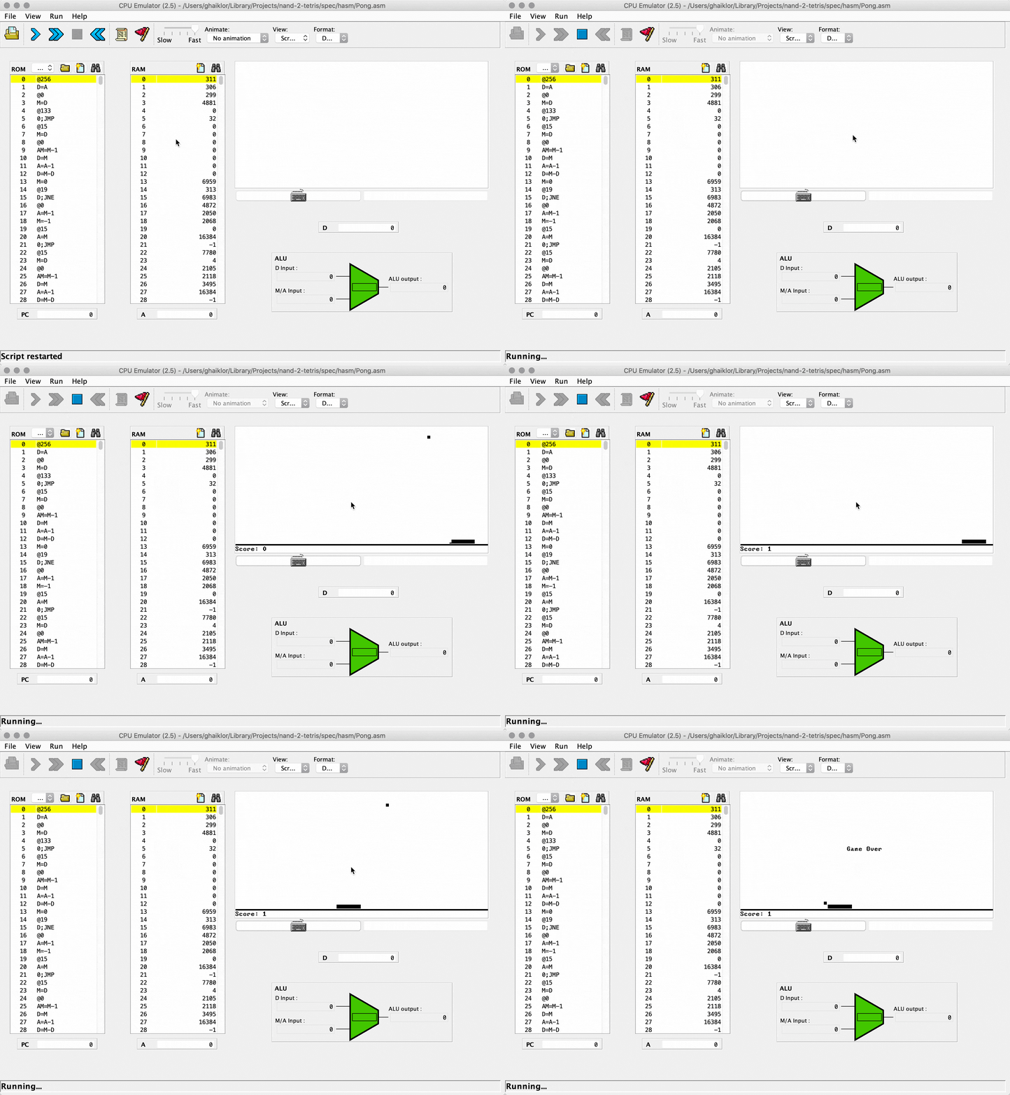
If you are interested in the crash course for “How does computers work”, read the article.
Boolean Logic
Let us start from the theory - from algebra. Before diving into CPU, gates and how they are implemented, you need to know more about boolean logic first.
The boolean logic is so important because we use it in building logical gates for the CPU, which are the building blocks for other features.
In boolean algebra, only two values are possible: true or false. We sometimes denote them as 1 or 0. Regarding operators in boolean algebra, there are three basic operators: conjunction (AND), disjunction (OR) and negation (NOT).
Let me give you examples of such expressions and operators:
- “It is rainy outside” can be evaluated as true or false. Well, if it is rainy outside, it is true; otherwise it is false, simple as that.
- “It is rainy outside AND I took an umbrella” both are expressions that can be evaluated to true or false, but the whole expression will be true, only if and only if “it is rainy outside” AND “you took an umbrella”. Otherwise, it will be false, even if you took an umbrella on a sunny day, or you didn’t on a rainy day.
- “It is rainy outside OR it is windy outside” can be true if it is rainy outside, or if it is windy outside, or both, rainy and windy, right? The only possibility when it is false is when the weather is neither rainy nor windy.
- “It is NOT rainy outside” is just a negation of the value. If it is rainy outside, then the expression is false and otherwise, if it is not rainy outside, is true.
There are also truth tables for these operators to denote the operands, operator and the result of the operator. Since in boolean algebra you can have only values 1 or 0, it is simple to write all the combinations of operands and their results in a pre-computed table.
For instance, the truth table for the AND operator with two operands has only four rows:
- 0 AND 0 = 0
- 0 AND 1 = 0
- 1 AND 0 = 0
- 1 AND 1 = 1
Why so much about boolean logic, you may ask. Because, when we will talk about gates in a minute, everything there will be about truth tables and a bit of engineering.
So, to recap. Boolean algebra has only two values: true, also denoted as 1, and false, also denoted as 0. It has operators AND, OR, NOT and you can apply them to the values. There are other logical operators that you can create by using those.
What has it to do with gates? Well, you may know that the crucial part of every electronic component is a transistor. These transistors can get a signal pass through them or “block” them.
This is how boolean logic maps to transistors. Boolean algebra has only two values: 1 or 0. While transistors can have only two states: pass the signal or not pass the signal. You can encode the transistor’s state into one-s and zero-s: pass the signal through if 1 and block it if 0.
Now, when we know enough about boolean logic, we can go forward and start talking about gates and hardware level.
NAND Gate
As for implementing theory in the real world, you are facing tough engineering issues. In our case, how can you implement the mechanism for some boolean operators?
Lucky for us, engineers have dealt with it. They implemented boolean operators NAND (NOT AND) or NOR (NOT OR) at the hardware level.
Also, it is proved that you can use NAND or NOR to build any boolean operator you’d like to. This property is called functional completeness. It means that you can use only NAND operator to create every logic gate by combining NAND gates in a network of gates - boolean expression.
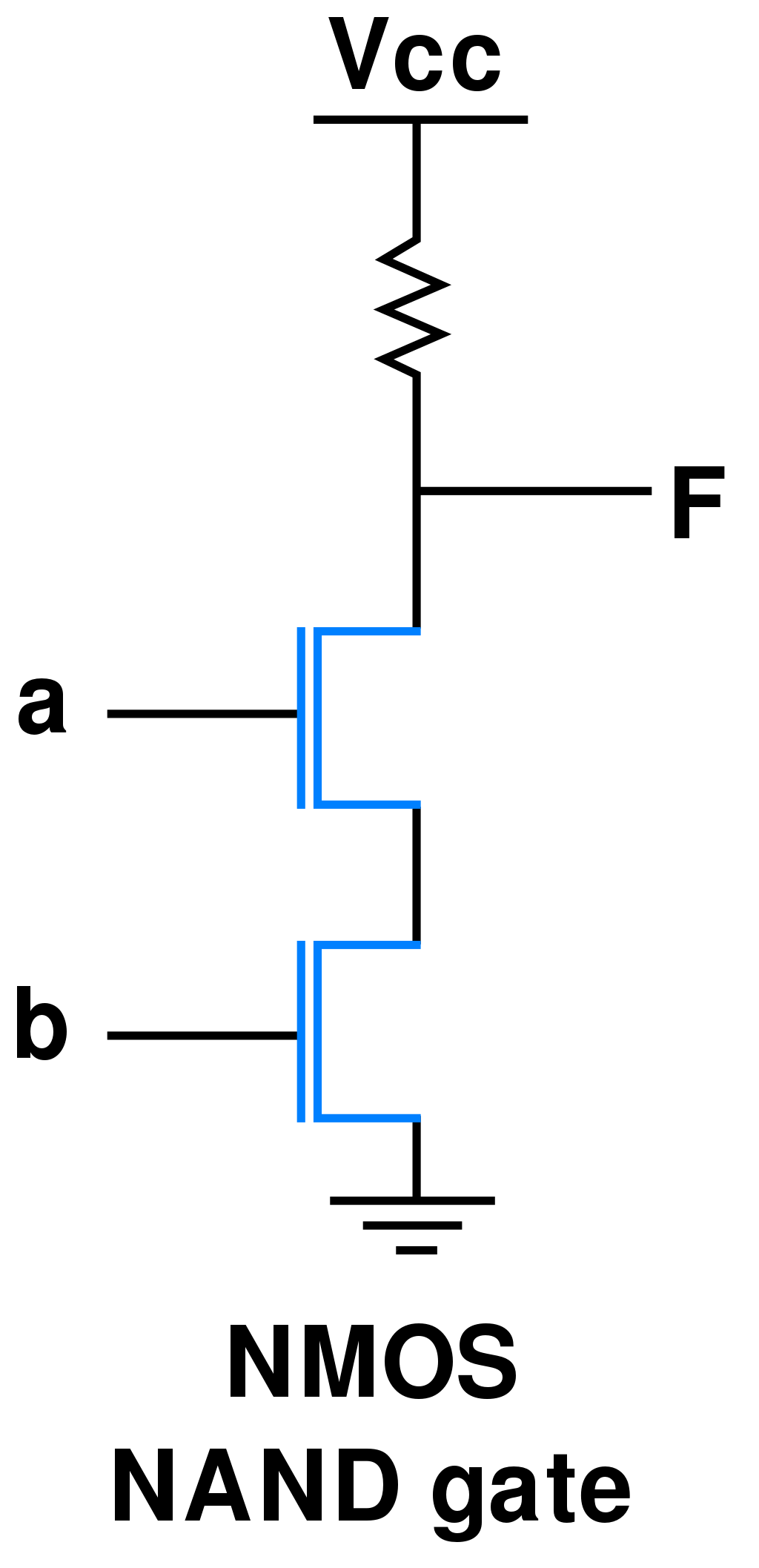
But how? Well, in case of NAND gate, engineers took two transistors (INPUT A, INPUT B) and combined them, that output signal (F) will be blocked if and only if two transistors are passing the signal to the ground (A = 1 AND B = 1). But, if either of transistors are not passing the signal to the ground (A = 0 OR B = 0), the signal will go to the output (F), emitting the signal, emitting the 1.
This way, they have implemented one of the boolean operators in a real world - NAND gate. Now, thanks to the functional completeness, you can use it to build other gates for other boolean operators, like AND, OR, XOR and so on and so forth.
I am not going into the technical details of those gates (there is a lot of material for a separate article), but so you know, every logical gate in the CPU implemented on top of basic gates like NAND or NOR.
Great! Thanks to these NAND gates, your CPU has logic gates for AND, OR, XOR, multiplexers and de-multiplexers (these are kind of conditional branching on hardware level).
But what about arithmetic in the CPU?
Arithmetic Logical Unit (ALU)
Often you want to calculate not only the logical expressions but also arithmetic expressions. Calculate not the 0 XOR 1, but what would be the result of 5 + 7?
This is when the arithmetic logical unit comes into play. But before we could calculate 5 + 7, we need to calculate the sum of two bits at least. We need to know how to calculate 0 + 1.
We can do that by implementing the half-adder. Half-adders take two inputs and emit two outputs: the sum of the inputs and the carry flag, in case if overflow happens to the next digit. If you ever did sums in column, you understand that I’m talking about carrying the overflow to the next digit.
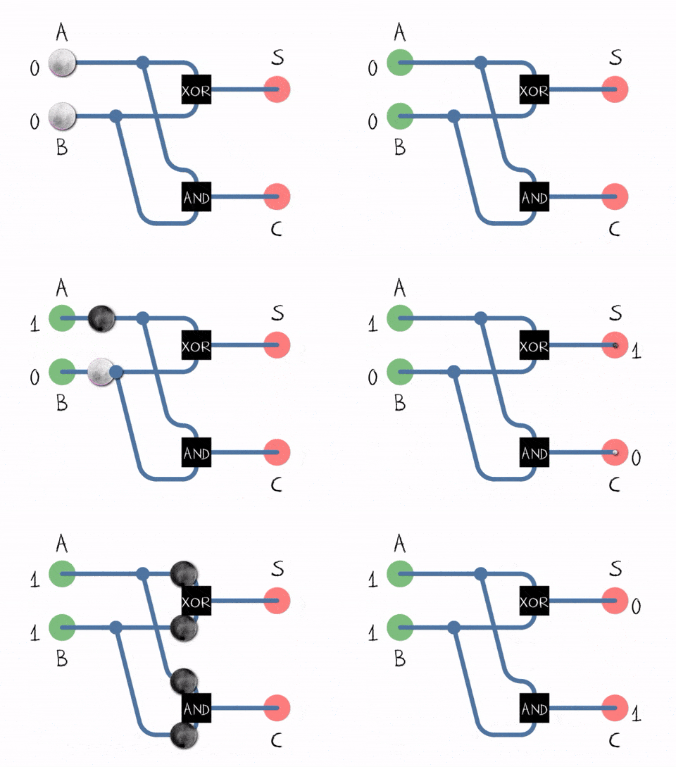
The truth table for the half adder:
- 0 + 0 = (S)um = 0, (C)arry = 0
- 0 + 1 = (S)um = 1, (C)arry = 0
- 1 + 0 = (S)um = 1, (C)arry = 0
- 1 + 1 = (S)um = 0, (C)arry = 1
Why 1 + 1 results into 0? Though carry is 1. It is because overflow happened. As we discussed before, boolean algebra has only zero-s and one-s. So you can encode the number by using two digits only. When you were summing up 1 + 1, it means 2, but there is no digit 2, so we need to carry it to the next digit, meaning, we set carry flag to 1.
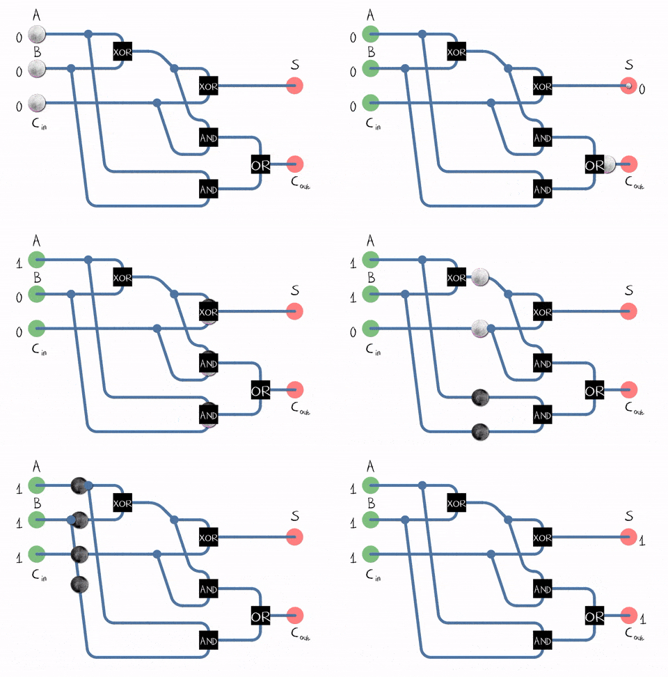
The problem with half adder is that it does not account for values carried in before. Full adder resolves the issue by introducing the third input, so we have inputs A and B that represents two digits and input C that represents the carry bit (did the overflow happened before).
Everything is great until we want to find out the sum of numbers greater than 0 or 1. Well, it is simple to implement by combining full adders in an array of them (each gate for each digit).
For instance, here is the array for summing up 4-digit binary numbers:
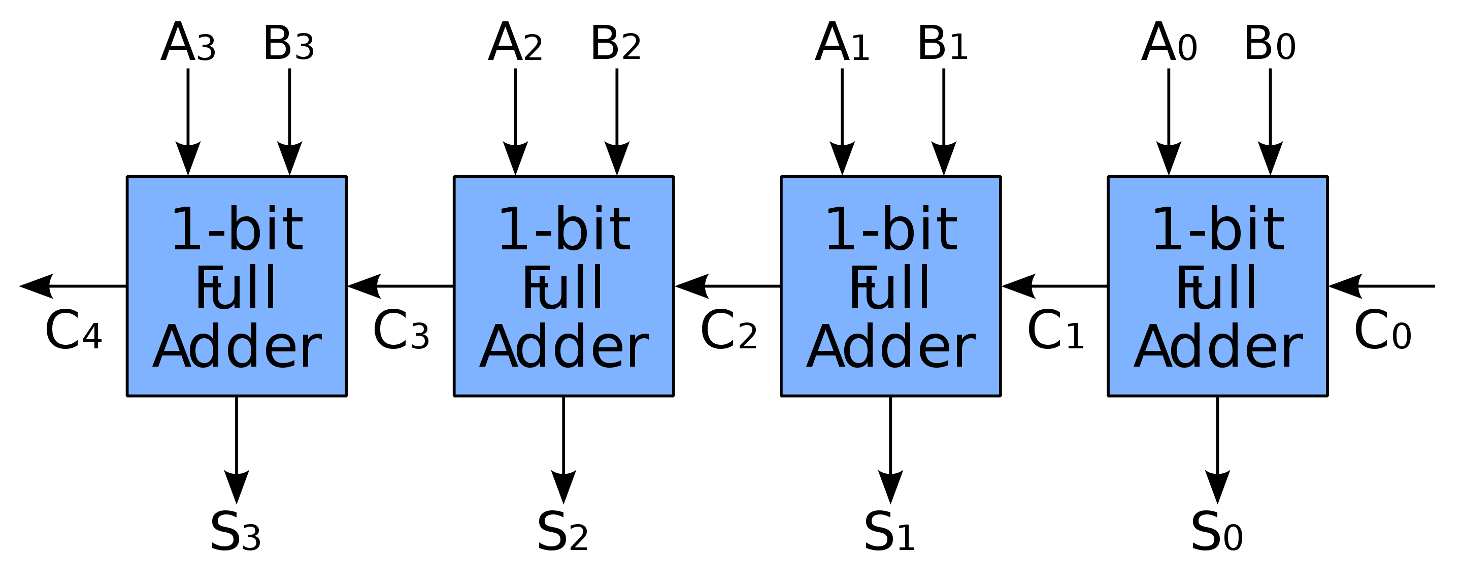
Now, you wanted to know the result of 5 + 7. 5 is 0101 in binary and 7 is 0111. Each of them has 4 digits, what we already have in an array of full adders!
You pass 0101 as A input and 0111 as a B input to the array of full adders and you will get another binary as the output, which will represent the sum of 5 + 7 in S output.
And it does all of that using logic gates we discussed before, cool, right?
The final part is the ALU itself. The ALU is a combinational circuit that performs arithmetic operations and built on top of adders we discussed above and a lot of logic gates so it can perform logic operations.
I will not explain the technical details about ALU implementation because it is very complex (to the article I’m writing right now). But I’ll tell you what it has as an input and what outputs.
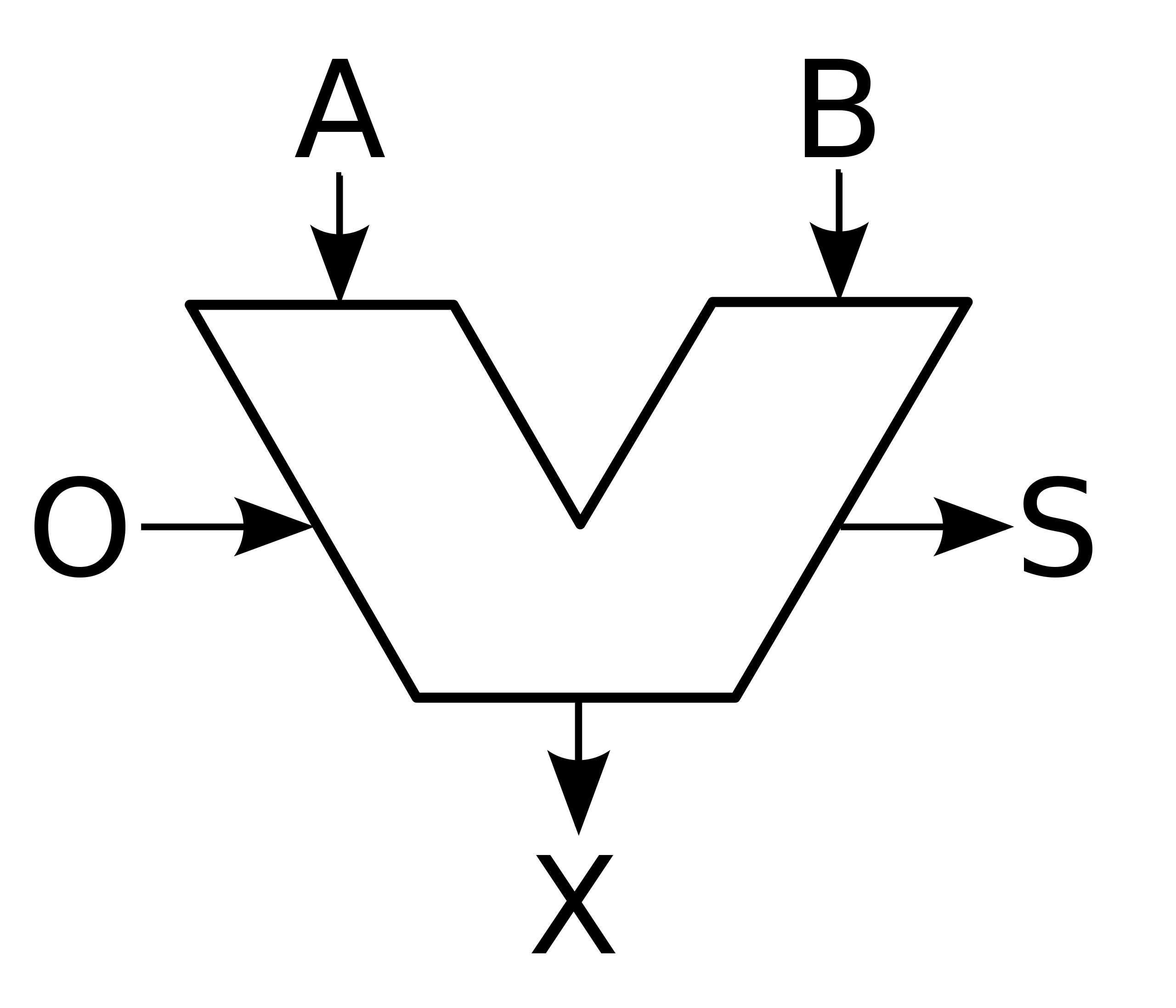
ALU has two inputs (A) and (B), that are represents the two numbers, two operands you want to work with. There is also another group of inputs (O) (opcode), by using this group of wiring, you can tell the ALU which operation you want to perform. Is that summing up? Or maybe you want to make logical AND?
ALU does the dirty job and emits two outputs: result of the operation (X) and the status (S). Status tells us if there is a negative result, or maybe overflow happened and so on.
To recap. We know what transistors are, how they are related to the boolean algebra and how we can implement it on a hardware level. Know how to implement arithmetic operators at the hardware level by using introduced logic gates and created adders. Built ALU on top of these adders and logic gates.
That’s already a lot to grasp, so we can close this part, which is called combinational chips. These are the chips that are based on boolean circuits and which are pure functions that calculate the result immediately, based on input.
Still, you can not use combinational chips to implement the mechanism for storing the information for further usage. So, how can we implement the mechanism for storing intermediate data without losing it? How can we implement memory?
Sequential Chips
When some changes in combinational chip wire happen, they react to these changes immediately. Meaning, while combinational chips work with present inputs only, sequential chips work with present and previous inputs in time.
Sequential chips, unlike combinational, have state, memory, history, call it whatever you like. That is the trick used for implementing the memory. Sequential chips are used to implement memory.
We will start with the simplest. How can one store one bit of information? How to store true or false? The answer is a flip-flop gate.
Flip-flop gate is used to capture the state of the chip. If the flip-flop is not in “update the state” mode - it does nothing, it just emits the same value it has already.
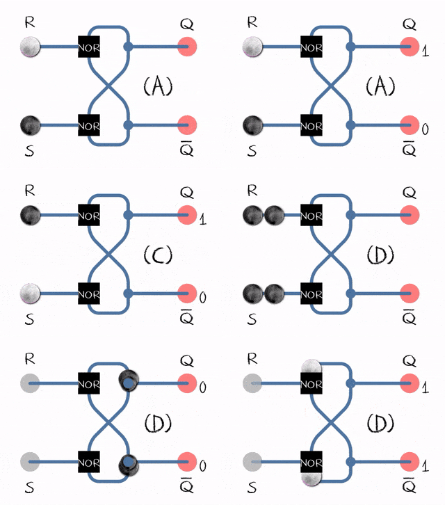
In the example to the right, there are two inputs (R)eset and (S)et and two outputs Q and complement of Q.
- (R)eset bit is set to 0 and (S)et bit to 1, it updates the flip-flop state to 1
- (R)eset bit is set to 1 and (S)et bit to 0, it updates the flip-flop to state 0
- Both bits (R)eset and (S)et are set to 0; it does nothing, just emits the value it already has
Now, let’s use the flip-flop and make an array of them.
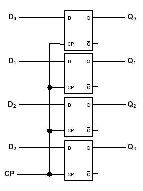
What about 4 flip-flops? That way, we could store 4 bits of information. Just make a register that has 4 inputs (D), each of the inputs connects to each flip-flop. The outputs of flip-flop connect to the outputs of the register (Q). Also, do not forget about resetting the state of our 4-bit register and connect the only input (CP) of the chip to all the (R)eset bits of each flip-flop in an array.
Looks like a working solution. Imagine, we want to store number 3 in the register. It is 0011 in binary. So, we are passing 0011 to each of the (D) inputs, that are connected to the (S)et bits of the flip-flop. Each of the flip-flop updates and emits 0011 as its outputs, which are connected to the (Q) outputs of the chip.
When you want to clear the register from number 3, you just pass a signal to (CP) input of your chip. It passes the signal to all the (R)eset bits of each flip-flop, leading to setting their value to 0 and so the output of your register to 0.
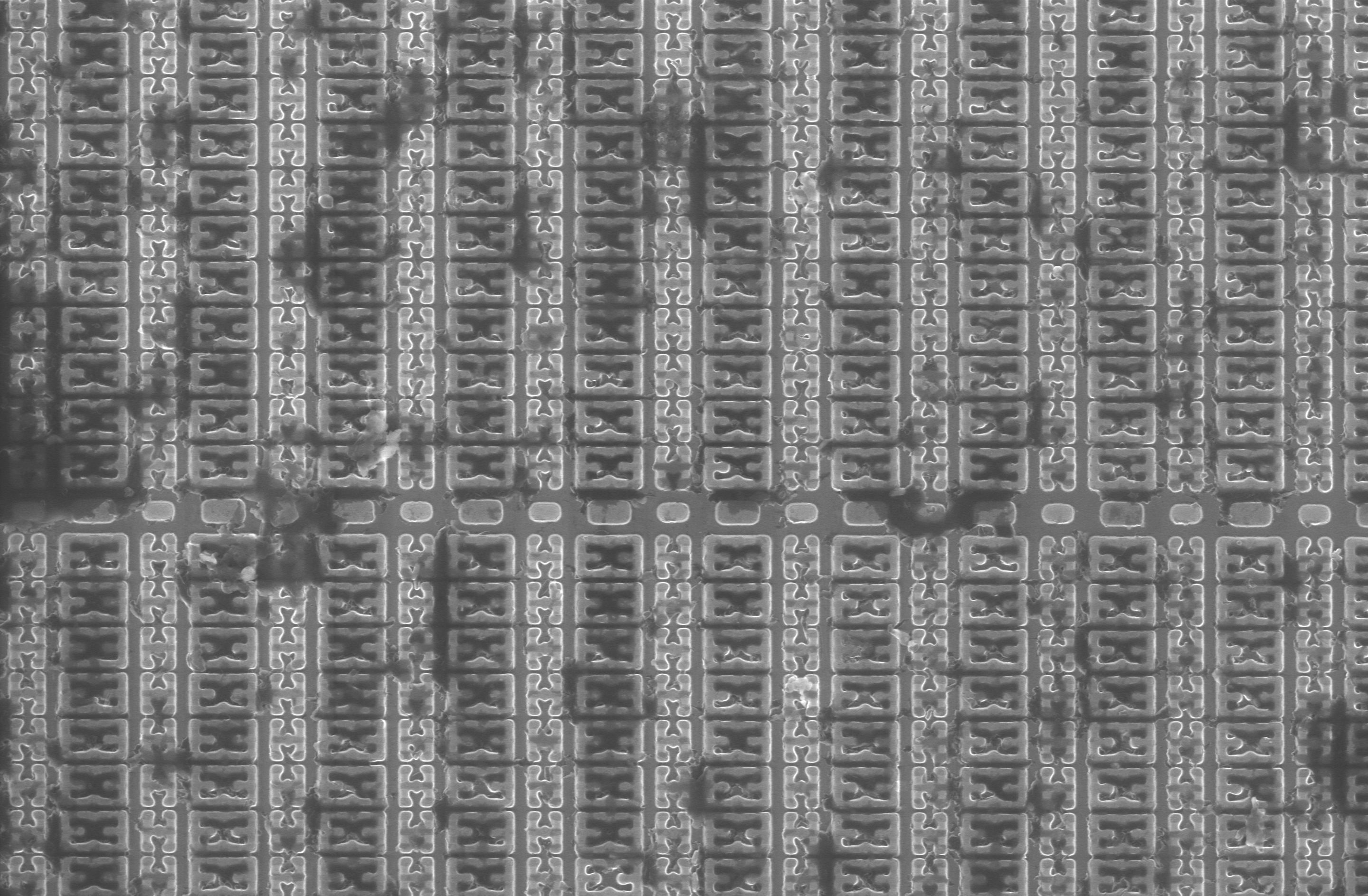
Now, imagine, that you have a lot, I mean, a lot of flip-flops in a huge array (like the one to the right).
Using logic gates (multiplexors and de-multiplexers) you can implement the addressing system on a hardware level. You can define the specific register you want to update by using the addressing system.
So, you tell the memory what register you want to update (address) and with what value. The addressing system takes the address of the register and uses it to “build a path” to it, using multiplexers. Everything else is the same as in our example with a 4-bit register.
To recap. We build memory on sequential chips that can store the state. One of them is a flip-flop gate that can store one bit of information. By using huge arrays of the flip-flops, you can implement the memory to hold Kb, Mb, and Gb of data.
The only missing detail right now is the software. I mean, we have a memory to store the binary data. We have an arithmetic logic unit that can do arithmetic and logic operations with that data. But how can we instruct it to do it?
Computer Architecture
Before diving into the answer for the question “How can we instruct the CPU to do something?”, I’d like to take a little historic detour and tell you about two noticeable men of their time. While I’ll be talking about them, we will come to the answer.
The first of them is Alan Turing, the man behind the Turing machine. You can read details about it by following the provided links (it is a lot to grasp, that is why I skip it here), but I’ll tell you the result of his research.
Alan Turing proved that if a programming language, CPU, automaton or whatever you can call a computable system has a Turing completeness property, it can simulate any other Turing machines. Meaning that you can program it to do any computable task.
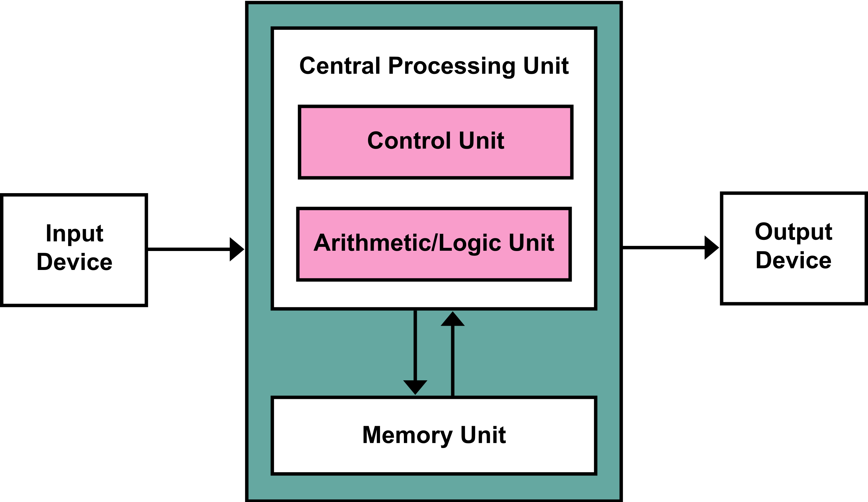
John von Neumann came up with the practical implementation of such systems. He designed an architecture for Turing complete digital computer and stated that it must comprise several components such as:
- Arithmetic logic unit and processor registers
- Memory that stored data and instructions for the machine
- Input and output for communication between the machine and its user
- Control unit that contains instruction register and program counter
So far, we have already discussed arithmetic and logic units and memory units before. But what we didn’t is a control unit. Because the control unit is the answer to the question, “How can we instruct the CPU to do something?”. As I promised, we came up to it.
Now, what is the control unit and how does it operate? It is complex because it wraps up all the parts we discussed before into one working thing. I can try to make a long story short and tell you that control unit uses “fetch-decode-execute” cycle to take your instructions, understand what the instruction is specified to do and, well, execute the instruction.
Yet, before the control unit could understand the instruction, we need to design its instruction set. Make an enumeration of instructions that CPU can execute.
For instance, I will take a simple instruction set used in the course nand2tetris. It has two types of instructions: computational instruction and “set the address” instruction, simple as that.
“Set the address” is an instruction that holds 16 bit, where most significant bit is 0 and the rest 15 bits are the address value - 0xxxxxxxxxxxxxxx. An example of such instruction is 0000000000000111. For the control unit, it means that it needs to update its address register to the value of 7 (0111 in binary).
Computational instruction is an instruction that is used to calculate arithmetic expressions, write results into registers, or make conditional jumps between instructions. The bit mask for this kind of instruction is 111accccccdddjjj. Where a is a modifier that shows from where we must take the value, from memory or from register. сссссс shows the opcode for ALU. ddd - which register we need to use for storing the result of operation. jjj - do we need to make conditional jumps to another instruction.
An example of such instruction will be 1110011111001000, meaning that it is the computational instruction, which instructs the control unit to take the value from register, increment it and the result write to the memory. We encode all of it into 16 bits. Can you imagine that?
So, the main idea of the instruction set is that the control unit must have designed instructions it can understand and execute.
Now, back to the “fetch-decode-execute” cycle:
- Control unit uses fetch stage to go into the memory unit and load the next instruction into the instruction register
- Decode stage breaks down the bits from the instruction and by manipulating them via logic gates sets the chips on the CPU to desired modes. Like, prepare register A for writing into or store the data from register back into memory, you got the idea
- Execute is the actual processing of the instruction. The result of the execution phase is the updated CPU/memory state.
It is a lot to grasp. It is ok if you didn’t get it the first time. I didn’t myself when I was going through the course. So, go through it again, take a cup of tea or coffee.
To recap, the CPU has a control unit that fetches the instructions from memory and executes them. These instructions must follow the instruction set architecture designed for the control unit they are running on.
Therefore, the whole program for the CPU is just a sequence of binary numbers, instructions, CPU must execute. Still, it will be very painful to write all these binary numbers by hand, right? You can’t remember neither all the instructions nor write them by hand. It will take a lot of time, at least.
That is why mnemonic instructions were born. Mnemonic instruction allows you to write human readable instruction, while another software can translate it back into binary code. The software that does this translation is called an assembler.
Assembler
From now on, I am not going into the technical details of implementation. Because it is the part where software only starts. To tell you all the details will take another thousands of words.
As we talked before, instructions for the CPU are a sequence of binary numbers, like 1110011111001000. It is hard to remember what each digit means if the same digit can have multiple meanings based on the value of other digits.
To resolve that, people came up with mnemonic instructions. They look like:
- mov eax, 5 - take a number 5 and (mov)e it to the register eax
- add eax, eax - take a number from register eax and (add) it to itself
- mov [8000], eax - take a number from register eax and (mov)e it to the memory by address 8000
- and so on and so forth…
Do you see the idea? While you could write the instructions to the CPU in binary, it is easier for you and others to read these instructions as if they were not binary but, well, more human readable.
We can translate these mnemonics one-to-one to binary code. By that, I mean that each mnemonic has one binary code to represent the instruction. That way, it is easier to implement the assembler - the software that translates mnemonics to their appropriate binary representation.
Let me show you an assembler in action by showing you mine assembler implemented during the course. What you see here is the assembly code, mnemonic instructions for the CPU, but when I pass it to the assembler, I got a binary code.
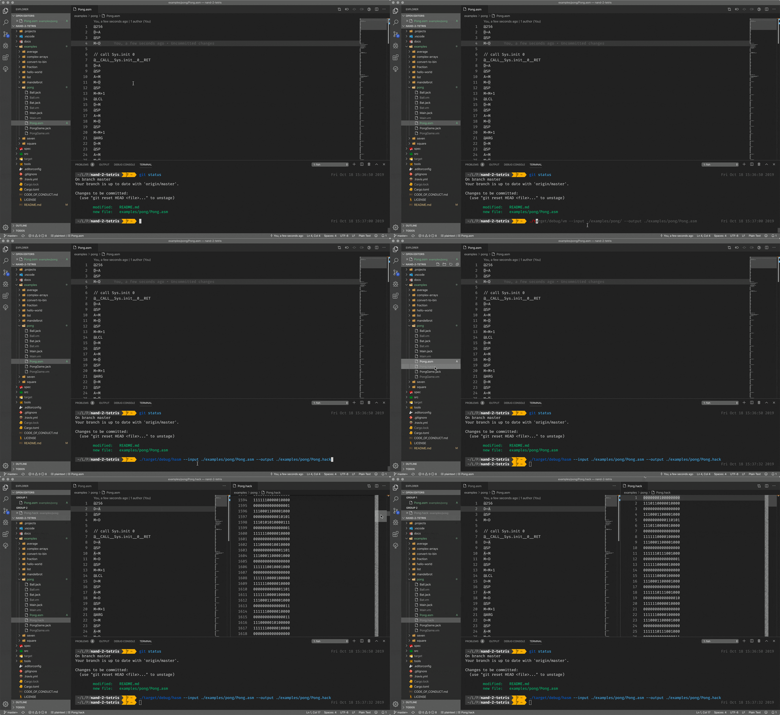
Having mnemonic instructions and the assembler, capable of translating such instructions back to the binary code, is a huge improvement in developer experience. But writing everything in assembly is a tough task.
That is why engineers came up with other ingenious ideas, and two of them are abstract stack machines and virtual machines.
Virtual Machine Translator
Imagine the following situation. You have 5 different CPU, each with a different instruction set. You need to write the program for these CPU. If you will write it in assembly for each of the CPU, it means that you need to write the same program 5 times from scratch (each CPU has its own instructions and assembler).
Now, imagine if there was a software, a virtual machine that has only one instruction set, but can be run on those 5 CPU. You could write code only once, for the virtual machine itself. Since we can run a virtual machine on those 5 CPU and interpret its instruction set, it will run the same code on different CPU. Meaning, you need to write code only once.
Basically, that is virtual machines in a few words. Their purpose is to abstract you from the underlying hardware.
One of them is a stack-based virtual machine. The core idea in such VMs is that everything is located on the stack and operators, functions, etc works with the stack only.
Since the location of the stack tip is an always known location in memory, it is easier to implement compilers/translators. In my case, I made a translator from stack-based code to the assembly. As you can see, there is a code with stack instructions, which will be translated to the assembly.
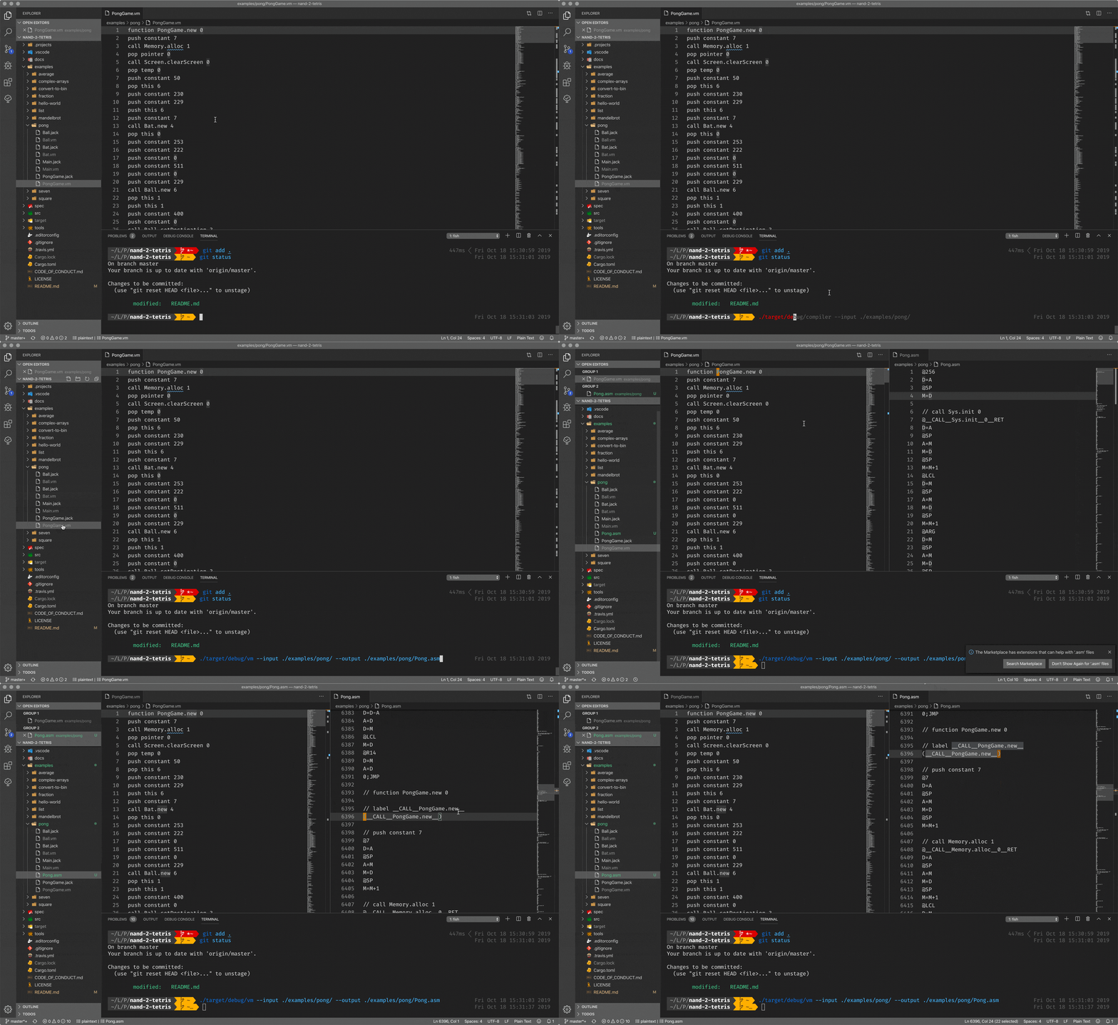
Stack-based code is another leap towards improving developer experience, but it is still not enough. It abstracts you from the underlying hardware so you can operate with the stack only, without knowing about some registers, memory, etc (almost) and it is great. But it is still pretty close to the hardware, and it is hard to call it a high-level programming language.
If we want to close the gap between developer experience and the actual running on the hardware, we need to implement the last thing from the chain - compiler for the high-level programming language.
Compiler
The purpose of the compiler is simple, but it is tough to implement. As an input to the compiler, you give a text, a source code of your program. The result is a new code, translated from your input, which can be run on a real hardware or some abstract machine.
There are a lot of compilers out in the world: cross-compilers, bootstrap compilers and so on and so forth. Though, what we did here during the course is just a compiler that compiles high-level language code to the stack-based code for our virtual machine, discussed before.
You can see a high-level language, with classes, methods, almost Java, I’d say. When we call the compiler with the input of the program, it compiles it to the stack-based code (on the right pane), for the virtual machine to run.
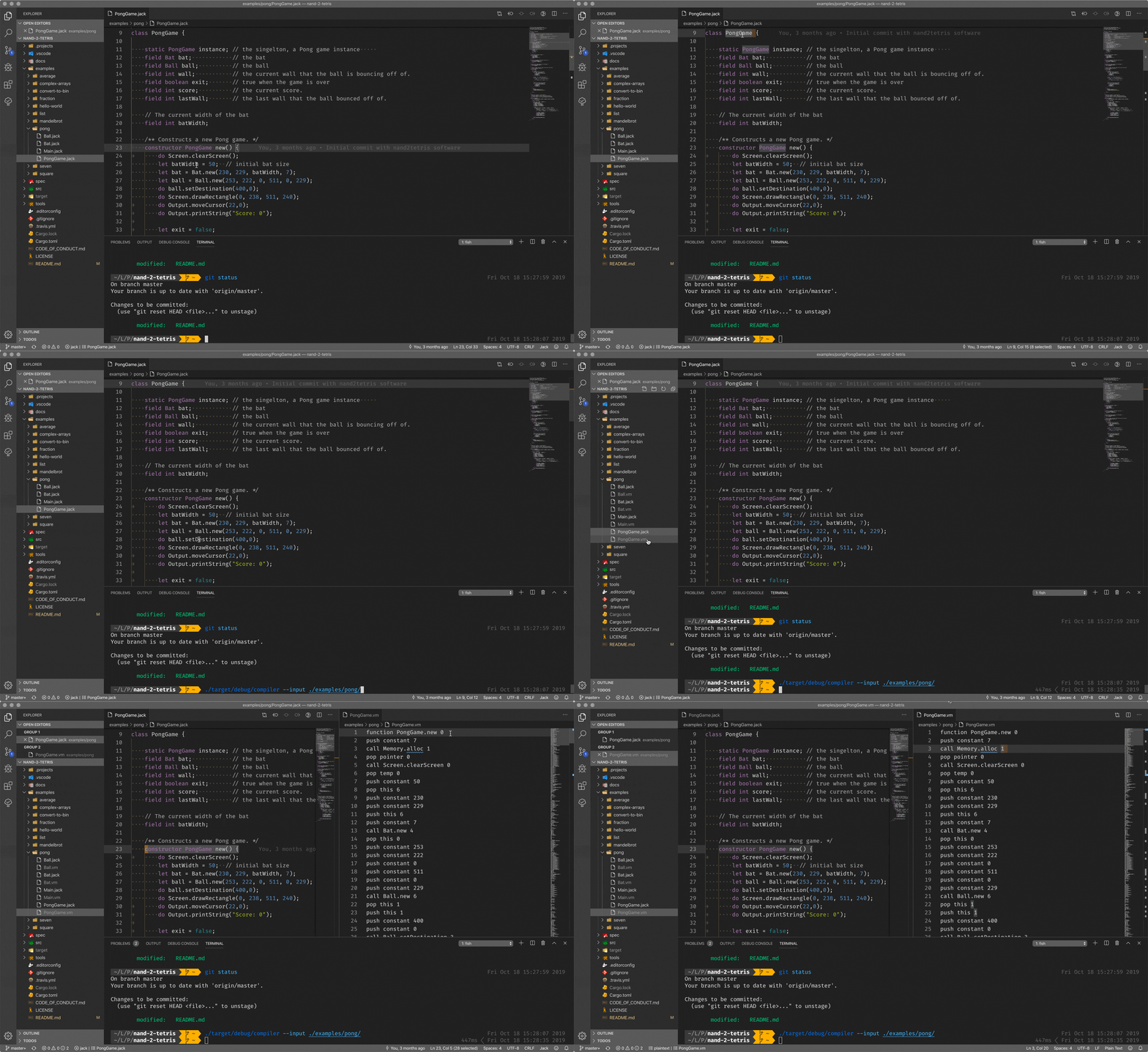
What compiler does not cover is hardware routines, like, allocate a block of memory, print something on the screen and so on and so forth. You could ask, who covers the gap between hardware routines and software routines?
Operating System
The operating system closes the gap between hardware and software.
When you are writing your code, you don’t think about “how to allocate memory for this variable” or “how can I print to the screen”. You just use it as granted and implicit.
That is because the compiler and operating system handles a lot of implicit things for you. For instance, when you are compiling some code with variables, the compiler injects calls to the operating system routines to allocate memory for the variables. It does it during the compilation process, so you not need to worry about it.
In the course, nand2tetris, we bootstrap the operating system on the Jack language. Language that you built with your own hands during the course, alongside with the compiler for it. It provides routine for operating the screen, keyboard, memory and alike.
So, when you call the method println or something, what is happening is a compiler translates it to the operating system routine call.
Well, we already covered too much for one article, so I offer to make a closing recap.
Recap
Let us assume that you have written an application and want to run it on the computer. Here is what happens next:
- Compiler takes the input as a source code of your application and emits another code capable of running on some abstract machines. Also, the compiler emits calls to the operating system for managing resources.
- The output of the compiler (stack-based code) is then passed to the virtual machine translator, which translates the code into assembly code.
- Assembly code goes to assembler, which translates mnemonic instructions to the binary numbers, that are instructions for the CPU.
- Control unit of the CPU fetches the instruction, decodes and executes it.
- While executing the instruction, the control unit communicates with the memory unit, which is based on flip-flop gates, and the arithmetic logic unit, which is based on adder gates.
- Every gate, flip-flop, adder and others are based on logic gates, like XOR, AND, and so on.
- We build each of the logic gates on top of the NAND or NOR gates, which is an implementation of boolean operators on a hardware level.
- NAND/NOR gates are implemented on top of transistors capable of passing the signal or blocking it.
That is the way your code is going through before it can start doing something.
Epilogue
If you are reading this, congratulations. You just came through the crash course on computers, starting from hardware to software.
I understand that there are a lot of missing parts, but the topic itself is huge also, do not forget that. Leave your thoughts and ideas in the comments, and I will update the article with more details.
Also, I recommend passing the course if you are interested in such things and always wanted to implement them yourselves. For me, the course took almost half a year, but I didn’t do it on a full-time basis.
Eugene Obrezkov, Software Engineer, Kyiv, Ukraine.


Comments